Silicon (Si)-metal (here Au and Ag) hybrid nanoscale objects with controlled dimension and desired morphology are exceptionally promising candidates for exploring the fundamental physics of small systems. The hetero-nanostructure of Si nanoparticle (NP) and Au/Ag NP is extremely important due to utilization of exciton-plasmon coupling. In Si NP-Au/Ag NP heterostructure, a modification in band structure is expected that leads to a complex and competitive decay dynamics of both excitons and plasmons. In this project, our primary aim is to probe the size-reduction-induced electronic state modification of ultra-small luminescent Si NPs and plasmonic noble metal (Au or Ag) NP individually by means of scanning tunneling microscopy (STM). The advantage of individual measurement is the ability to determine the exact correlation between their size and intrinsic property modification.
For example, the photoluminescence (PL) from Si NP offers different potential applications in optoelectronic devices though mechanism of PL from Si NP is still controversial. The bottleneck in determining the exact reasons behind the optical emission is the lack of knowledge of the detailed energy spectrum and the electronic transport through Si NP. In this regard, the study of the scanning tunneling spectroscopy of individual NP is a comprehensive tool in determining the transparency of the tunnel barriers and mapping local density of states.
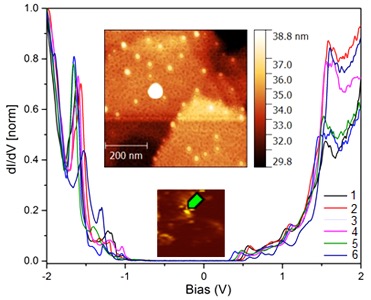
Figure 1 exhibits such a single particle measurement by STM of Si NP in the dimension ~5 nm, whereas the inset in the figure shows uniform dispersion of Si NP. A single Si NP between the tip of the STM and the conducting substrate forms a double barrier tunnel junction. In the picture, a clear Coulomb blockade has been observed which has a direct co-relation with the size of the NP. The various kinks beside the Coulomb blockade region demonstrate the electronic transport and bandgap modification of Si NP.
This type of study is interesting for engineering the electronic bandgap and the electronic state of the individual NP. By proper engineering and integration with other nanomaterials (especially a noble metal), it is possible to envisage future optoelectronic devices, energy harvesting materials, and sensing materials at nanoscale.
Information
Contributors: T. S. Basu
External cooperations: J. Demsar, Intitut für Physik, Johannes Gutenberg Universität Mainz; A. Zumbusch, Fachbereich Chemie, Universität Konstanz
Fundings: Alexander von Humboldt-Foundation; Zukunftskolleg Universität Konstanz
Period: 2015 - 2018