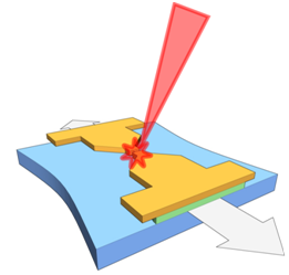
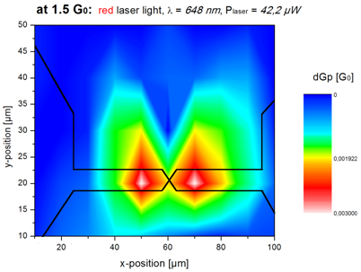
In this project we investigate the influence of laser light onto the electric conductance of an atomic-sized contact made of metal. These contacts are realized with the mechanically break junction technique. Recent works showed that upon illumination with laser light the electric conductance of such a contact increases and depends on the point of illumination. The maximum increase in conductance is found at different points of illumination for different wavelengths. For red light it was found that the maximum in change of conductance is observed while illuminating the metal leads which are pointing towards the atomic-sized contact (picture). These findings give rise to the idea that, aside from pure thermal effects, also surface plasmons might contribute to the conductance of an atomic-sized contact.
Currently we are working on performing the experiment inside a cryostat at about 1.5 K. Additionally the time resolution will be enhanced to be able to distinguish between thermal and non-thermal effects.
Simultaneously it is necessary to investigate the propagation of surface plasmons across a nano-contact or even gaps in the metal. For that purpose surface plasmons are excited by a focused laser beam hitting a grating structure in a microscope setup. Further gratings on both sides of a nano-contact allow tracking the propagation of the surface plasmons. The results of the measurements are compared to computer simulations made by FDTD.
Publications
- Ghafoori G, Boneberg J, Leiderer P, Scheer E. Opt Express. 2016 Jul 25;24(15):17313-20. doi: 10.1364/OE.24.017313.
- GHAFOORI, Golaleh, 2016. Guiding light to nano-constrictions : excitation and propagation of Surface Plasmon Polaritons on nano-patterened metal films
- BÄDICKER, Matthias, 2016. Zeitabhängige Leitwertänderung eines atomaren Kontaktes bei Beleuchtung mit Laserlicht
- BENNER, Daniel, Johannes BONEBERG, Philipp NÜRNBERGER, Golaleh GHAFOORI, Paul LEIDERER, Elke SCHEER, 2013. Transmission of surface plasmon polaritons through atomic-size constrictions. In: New Journal of Physics. 15(11), 113014. ISSN 1367-2630. eISSN 1367-2630
- KOLLOCH, Andreas, Daniel BENNER, Matthias BÄDICKER, Reimar WAITZ, Tobias GELDHAUSER, Johannes BONEBERG, Paul LEIDERER, Elke SCHEER, 2011. Characterization and applications of plasmon fields in metal nanostructures. Smart Nano-Micro Materials and Devices. Melbourne, Australia. In: JUODKAZIS, Saulius, ed., Min GU, ed.. Smart Nano-Micro Materials and Devices. Smart Nano-Micro Materials and Devices. Melbourne, Australia. SPIE, pp. 820404
Information
Contributors: T. Möller
Former contributors: M. Bädicker, G. Ghafoori, D. Benner, R. Waitz